While upgrading the memory (RAM) of my notebook I did a lot of study as to what exact kind of RAM would my notebook use without problems. By the end, while I finalized on what RAM I need for my notebook, I had compiled a small document on Basic RAM Information courtesy Crucial® FAQs.
I hope this guide to be helpful to you but with no warranty though. :-)
Do I have to buy the same size upgrade as the memory module currently
installed in my computer or can I mix different sizes?
In newer systems using SDRAM or DDR SDRAM memory, you can use modules of different densities with no problem. For example, if your computer came with a 128MB memory module, you can add a 256MB module for a total of 384MB of RAM. However, if you have a “dual-channel” system and want to take advantage of that technology, you will need to ensure that the modules in each memory slot are the same density.
Can I mix and match speeds?
Rather than give memory modules catchy names, modules are referred to by their specifications. If you don’t know a lot about memory, the numbers can be confusing. Here’s a short summary of the most popular types of memory and what the numbers refer to.
DDR PC1600, PC2100, PC2700, and PC3200 (DDR400)
In DDR modules, the numbers that come after the “PC” refer to the total
bandwidth of the module. For this type of memory, a higher number represents
faster memory, or more bandwidth. Occasionally DDR is referred to as “DDR400”
or “DDR333,” for example. When written this way, the numbers after “DDR” refer
to the data transfer rate of the components.
PC1600 memory is DDR designed for use in systems with a 100-MHz front-side bus, (providing a 200 mega transfers per second (MT/s) data transfer rate). The “1600” refers to the module’s bandwidth (the maximum amount of data it can transfer each second), which is 1.6 GB. PC1600 has been replaced by PC2100, which is backward compatible.
PC2100 memory is DDR designed for use in systems with a 133-MHz front-side bus (providing a 266 MT/s data transfer rate). The “2100” refers to the module’s bandwidth (the maximum amount of data it can transfer each second), which is 2.1 GB. PC2100 is used primarily in AMD Athlon systems, Pentium III systems, and Pentium IV systems.
PC2700 memory is DDR designed for use in systems with a 166-MHz front-side bus (providing a 333 MT/s data transfer rate). The “2700” refers to the module’s bandwidth (the maximum amount of data it can transfer each second), which is 2.7 GB.
PC3200 (commonly referred to as DDR400) memory is DDR designed for use in systems with a 200-MHz front-side bus (providing a 400 MT/s data transfer rate). The “3200” refers to the module’s bandwidth (the maximum amount of data it can transfer each second), which is 3.2 GB.
**SDRAM PC100 and PC133 **
In SDRAM modules, the numbers that come after the “PC” refer to the speed of
the system’s front side bus.
PC100 memory is SDRAM designed for use in systems with a 100-MHz front-side bus. It is used in many Pentium II, Pentium III, AMD K6-III, AMD Athlon, AMD Duron, and Power Mac G4 systems.
PC133 memory is SDRAM designed for use in systems with a 133-MHz front-side bus. It is used in many Pentium III B, AMD Athlon, and Power Mac G4 systems.
**Older memory technology such as PC66 SDRAM, FPM, and EDO **
PC66 memory is SDRAM designed for use in systems with a 66-MHz front-side bus.
It is used in the Pentium 133-MHz systems and Power Macintosh G3 systems.
FPM and EDO speeds are written in nanoseconds (ns), which indicates their access time; the lower the number, the faster the memory (it takes fewer nanoseconds to process data).
It may seem confusing, but faster memory will not necessarily make your system faster. You can’t speed up your computer by adding faster memory if other components in your computer (your processor or other memory modules) operate at a slower speed.
Keep in mind, that the right memory for your computer is the kind of memory it was designed to take. Check your system manual or look up your system in the Crucial Memory Advisor to find the memory guaranteed to be 100 percent compatible or your money back!
What is the difference between PC2100 (DDR266), PC2700 (DDR333), and PC3200
(DDR400)?
PC2100 (DDR266) memory, PC2700 (DDR333) memory, and PC3200 (DDR400) memory are all types of Double Data Rate (DDR) SDRAM. The varying numbers refer to the different speeds of memory your computer was designed for.
Let’s take a look at PC2100 (DDR266) to break it down simply.
PC2100 refers to the bandwidth of the memory. A PC2100 module has the bandwidth of 2.1GB/sec therefore it is referred to as PC2100.
DDR266 refers to the effective front-side bus speed of your system. While your DDR system or motherboard may operate a 133MHz front-side bus, its effective front-side bus speed is 266MHz because DDR effectively doubles the amount of data transferred per cycle that a non-DDR system would.
The same holds true for PC2700 (DDR333) which has a bandwidth of 2.7GB/sec and is designed for use in systems and motherboards which require a 166MHz front- side bus, with an effective front-side bus speed of 333MHz.
PC3200 DDR (DDR400) has a bandwidth of 3.2GB/sec and is designed for use in systems and motherboards which require a 200MHz front-side bus with an effective front-side bus speed of 400MHz.
Though DDR memory was designed to be backward compatible (meaning you can use PC3200 DDR in a computer designed to use PC2100 DDR or vice-versa), we always recommend that you use the Crucial Memory Selector to find exactly the right memory for your computer.
My computer uses PC2700 (DDR333). Can I use PC3200 (DDR400)?
DDR memory was designed to be backward compatible so generally speaking, you can safely add faster memory to your computer. For example, you can install a PC3200 DDR module in a computer that calls for PC2700 DDR. However, keep in mind that faster memory will not necessarily make your system faster. You can’t speed up your computer by adding faster memory if other components in your computer (your processor or other memory modules) operate at a slower speed.
The right memory for your computer is the kind of memory it was designed to take. Check your system manual or look up your system in the Crucial Memory Advisor to find the memory guaranteed to be 100 percent compatible or your money back.
What is dual-channel DDR memory?
The terminology “dual-channel memory” is being misused by some in the memory industry, which can mislead the consumer. The fact is there’s no such thing as dual-channel memory. There are, however, dual-channel platforms.
When properly used, the term “dual channel” refers to the DDR or DDR2 chipset on certain motherboards designed with two memory channels instead of one. The two channels handle memory-processing more efficiently by utilizing the theoretical bandwidth of the two modules, thus reducing system latencies, the timing delays that inherently occur with one memory module. For example, one controller reads and writes data while the second controller prepares for the next access, hence, eliminating the reset and setup delays that occur before one memory module can begin the read/write process all over again. Think of it like two relay runners. The first runner runs one leg while the second runner sets up and prepares to receive the baton smoothly and carry on the task at hand without delay. While performance gains from dual-channel chipsets aren’t huge, they can increase bandwidth by as much as 10 percent. To those seeking to push the performance envelope, that 10 percent can be very important.
So the next time you come across a product that’s touted and sold as dual- channel memory, know this- It’s simply two DDR or DDR2 memory modules, packaged and marketed as a specialty product or a must-have “kit.” If indeed you have a dual-channel platform and you want to take advantage of the performance gain it offers, our advice is to opt for high quality and service over expensive packaging, and simply purchase your DDR or DDR2 memory in pairs. However, be very careful to order two modules with the exact same specifications; the modules must be identical to each other to perform correctly.
How much RAM can Windows handle?
That depends on two factors: the amount of memory your computer can handle, and the amount of memory your Windows operating system (OS) can handle.
First, your computer is designed to hold a maximum amount of RAM. When you look up your computer in the Memory Selector, you will see the system maximum on the page that lists the compatible upgrades for your system.
Second, the OS maximum, is the maximum amount of memory that your particular version of Windows, Linux, or Mac OS can handle.
When purchasing your memory upgrade, ensure you do not exceed the lower of the two maximums (OS & computer maximums.) Too much RAM can lower your system’s performance or cause other problems. (In most cases, the system maximum is lower than the OS maximum.)
Here are the OS maximums for popular versions of Microsoft Windows.
Windows 95: 1GB
Windows 98: 1GB
Windows 98SE: 1GB
Windows ME: 1.5GB
Windows NT: 4GB
Windows 2000 Professional: 4GB
Windows 2000 Advanced Server: 4GB or 8GB with PAE enabled
Windows 2000 Datacenter Server: 4GB or 64GB with PAE enabled
Windows XP Home: 4GB
Windows XP Professional: 4GB
Here are the maximums for some other platforms.
OS X: 8GB due to current hardware limitations
OS 9.x: 1.5GB (no single application can utilize more than 1GB)
Linux: 64GB
How can I “max out” the memory on my computer?
Once you have found your computer in the Crucial Memory Advisor™ tool, locate the maximum memory capacity and number of memory slots for your particular computer. Generally speaking, you can determine the largest memory module each slot can take by dividing the maximum capacity by the total number of slots. For example, if your computer has a maximum memory capacity of 2048MB (i.e. 2GB), and has two slots, the largest module you can install in each slot is a 1GB memory module.
However, there are exceptions to this general rule. For example, there are situations where a computer with 4 memory slots and a 2GB maximum memory capacity will accept two 1GB modules. There are also times when a system would only accept a 512MB module at launch, but down the road would take a 1GB module with a BIOS upgrade. This is why it is so important to use the Crucial Memory Advisor™ tool which can alert you to these exceptions.
To completely “max out” the memory on your computer, you may need to actually remove memory modules currently installed and replace them with larger- capacity modules. Using the example above, if your computer has one 512MB module already installed, with one memory slot open, you would need to remove the 512MB and install two 1GB modules to truly “max out” your computer.
The System Scanner results showed my computer’s front side bus speed is
200MHz but it’s supposed to be 800MHz. What’s wrong?
Many newer computers use double data rate or “quad-pumped” front side busses. While the actual front side bus frequency is 200MHz, the enhanced capability of your computer’s front side bus allows it to perform like a 400MHz or 800MHz front side bus.
More Assistance
I have 256MB of memory, but the Crucial System Scanner only shows 248MB.
What happened to the missing memory?
Quite a few computers, especially notebook computers and budget desktop computers, use integrated graphics processors that share memory with the main system memory. As a result, your computer will set aside a portion of the main system memory for the integrated graphics processor, reducing the actual amount of memory available to the rest of your computer. This amount can range from as low as 8MB to as high as 128MB, depending on your computer’s specific configuration. While some computers allow you to adjust how much memory the graphics processor uses, there is no way of preventing this from happening, short of installing a graphics card with dedicated memory for the graphics processor.
Rambus® and DDR Explained
DDR SDRAM
DDR (double data rate) memory is the next generation SDRAM. Like SDRAM, DDR is
synchronous with the system clock. The big difference between DDR and SDRAM
memory is that DDR reads data on both the rising and falling edges of the
clock signal. SDRAM only carries information on the rising edge of a signal.
Basically this allows the DDR module to transfer data twice as fast as SDRAM.
For example, instead of a data rate of 133MHz, DDR memory transfers data at
266MHz.
DDR modules, like their SDRAM predecessors, are called DIMMs. They use motherboard system designs similar to those used by SDRAM; however, DDR is not backward compatible with SDRAM-designed motherboards. DDR memory supports both ECC (error correction code, typically used in servers) and non-parity (used on desktops/laptops.)
If your system or motherboard requires DDR, you can purchase the upgrades you need through Crucial’s Memory Selector™. For more information on DDR, see the DDR Shopping Guide.
Rambus DRAM
Rambus memory (RDRAM®) is a revolutionary step from SDRAM. It’s a memory
design with changes to the bus structure and how signals are carried. Rambus
memory sends less information on the data bus (which is 16 or 18 bits wide as
opposed to the standard 64 or 72 bits) but it sends data more frequently. It
also reads data on both the rising and falling edges of the clock signal, as
DDR does. As a result, Rambus memory is able to achieve effective data
transfer speeds of 800MHz and higher.
Another difference with Rambus memory is that all memory slots in the motherboard must be populated. Even if all the memory is contained in a single module, the “unused” sockets must be populated with a PCB, known as a continuity module, to complete the circuit.
Rambus DRAM modules are known as RIMM™ modules (Rambus inline memory modules). Rambus memory supports both ECC and non-ECC applications.
Production Challenges
One of the challenges Rambus memory faces is that it is expensive to produce
compared to SDRAM and DDR. Rambus memory is proprietary technology of Rambus
Inc. Manufacturers that want to produce it are required to pay a royalty to
Rambus Inc., whereas DDR designs are open architecture. Other cost factors for
Rambus memory include additional module manufacturing and testing processes
and a larger die size. Rambus die (chips) are much larger than SDRAM or DDR
die. That means fewer parts can be produced on a wafer.
Performance
Now for the million-dollar question: How do DDR and Rambus memory compare
performance wise? Sorry, I know you don’t want to hear this – that depends.
Both technologies have their own ardent supporters and we have seen several
different benchmarks to date that provide conflicting results.
On the surface, it seems simple: Data flow at 800MHz is faster than data flow at 266MHz, right? Unfortunately, it isn’t that simple. While Rambus modules may have the ability to transfer data faster, it appears to have higher latency (the amount of time you have to wait until data flows) than that of a DDR system. In other words, the first data item transferred in a Rambus transaction takes longer to initiate than the first data item moved in a DDR system. This is due in part to how the systems are constructed.
In a DDR or SDRAM system, each DIMM is connected, individually and in parallel, to the data bus. So whether you have a single DIMM or multiple DIMMs, the amount of time it takes to initiate a data transfer is effectively unchanged.
In a Rambus system, RIMM modules are connected to the bus in a series. The first data item transferred must pass through each RIMM module before it reaches the bus. This makes for a much longer distance for the signal to travel. The result is higher latency. That’s not necessarily a problem in an environment where data transactions involve lengthy streams of data, such as gaming. But it can become an issue in environments where many small transactions are initiated regularly, such as a server.
To further explain, here’s an example that we can all relate to – driving your car to the store. You can take the roundabout freeway and drive 20 miles at 70 MPH. Or, you can take a more direct route and drive just 5 miles at 50 MPH. You might go faster on the freeway but you’ll get to the store (Memory Controller) faster on the straight-line route.
Bottom Line
Generally speaking, motherboards are built to support one type of memory. You
cannot mix and match more than one type of SDRAM, DDR, or Rambus memory on the
same motherboard in any system. They will not function and will not even fit
in the same sockets. The right type of memory to use is the one that your
motherboard takes! And no matter what type of memory you use, more is
typically better. A memory upgrade is still one of the most cost-effective
ways to improve system performance.
Micron manufactures memory - Here’s how!
Memory chips are integrated circuits with various components (transistors, resistors, and capacitors) formed on the same chip. These integrated circuits begin as silicon, which is basically extracted from sand. Turning silicon into memory chips is an exacting, meticulous procedure involving engineers, metallurgists, chemists and physicists.
Memory is produced in a very large facility called a fab, which contains many cleanroom environments. Semiconductor memory chips are manufactured in cleanroom environments because the circuitry is so small that even tiny bits of dust can damage it. Micron’s Boise facility covers over 1.8 million square feet and has class 1 and class 10 cleanrooms. In a class 1 cleanroom, there is no more than 1 particle of dust in a cubic foot of air. In comparison, a clean, modern hospital has about 10,000 dust particles per cubic foot of air. The air inside a cleanroom is filtered and recirculated continuously, and employees wear special clothing such as dust-free gowns, caps, and masks to help keep the air particle-free. This special clothing is commonly referred to as a bunny suit.
The first step from silicon to integrated circuit is the creation of a pure,
single-crystal cylinder, or ingot, of silicon six to eight inches in diameter.
These cylinders are sliced into thin, highly polished wafers less than one-
fortieth of an inch thick. Micron uses six- and twelve-inch wafers in its
fabrication processes. The circuit elements (transistors, resistors, and
capacitors) are built in layers onto the silicon wafer. 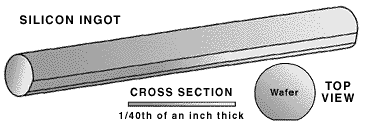
Most chip designs are developed with the help of computer systems or computer- aided design (CAD) systems. Circuits are developed, tested by simulation, and perfected on computer systems before they are actually built. When the design is complete, glass photomasks are made�one mask for each layer of the circuit. These glass photomasks are used in a process called photolithography.
In the sterile cleanroom environment, the wafers are exposed to a multiple- step photolithography process that is repeated once for each mask required by the circuit. Each mask defines different parts of a transistor, capacitor, resistor, or connector composing the complete integrated circuit and defines the circuitry pattern for each layer on which the device is fabricated.
Memory Chip Manufacturing Part 2
A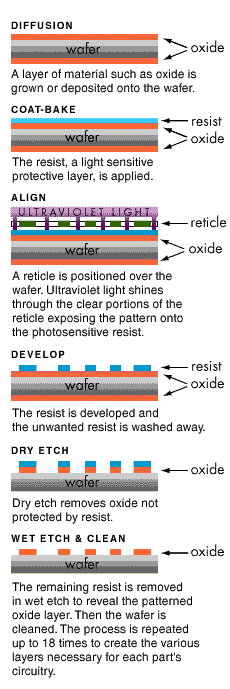 t the beginning
of the production process, the bare silicon wafer is covered with a thin glass
layer followed by a nitride layer. The glass layer is formed by exposing the
silicon wafer to oxygen at temperatures of 900 degrees C or higher for an hour
or more, depending on how thick a layer is required. Glass (silicon dioxide)
is formed in the silicon material by exposing it to oxygen. At high
temperatures, this chemical reaction (called oxidation) occurs at a much
faster rate.
t the beginning
of the production process, the bare silicon wafer is covered with a thin glass
layer followed by a nitride layer. The glass layer is formed by exposing the
silicon wafer to oxygen at temperatures of 900 degrees C or higher for an hour
or more, depending on how thick a layer is required. Glass (silicon dioxide)
is formed in the silicon material by exposing it to oxygen. At high
temperatures, this chemical reaction (called oxidation) occurs at a much
faster rate.
Next, the wafer is uniformly coated with a thick light-sensitive liquid called photoresist. Portions of the wafer are selected for exposure by carefully aligning a mask between an ultraviolet light source and the wafer. In the transparent areas of the mask, light passes through and exposes the photoresist.
Photoresist undergoes a chemical change when exposed to ultraviolet light. This chemical change allows the subsequent developer solution to remove the exposed photoresist while leaving the unexposed photoresist on the wafer. Wafers are exposed to a multiple-step photolithography process that is repeated once for each mask required by the circuit.
The wafer is subjected to an etch process (either wet acid or plasma dry gas etch) to remove that portion of the nitride layer that is not protected by the hardened photoresist. This leaves a nitride pattern on the wafer in the exact design of the mask. Hundreds of memory chips can be etched onto each wafer. The hardened photoresist is then removed (cleaned) with another chemical.
Dopants are frequently introduced as part of the layer formation in high temperature diffusion operations or with ion implanters. These dopants tailor the silicon’s conductive characteristics making it either negative (n-type) or positive (p-type). These basic steps are repeated for additional layers of polysilicon, glass, and aluminum.
The finished wafer is an intricate sandwich of n-type and p-type silicon and insulating layers of glass and silicon nitride.
Memory Chip Manufacturing Part 3
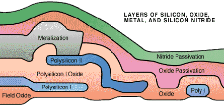
All of the circuit elements (transistor, resistor, and capacitor) are constructed during the first few mask operations. The next masking steps connect these circuit elements together.
An insulating layer of glass (called BPSG) is deposited and a contact mask is used to define the contact points or windows of each of the circuit elements. After the contact windows are etched, the entire wafer is covered with a thin layer of aluminum in a sputtering chamber.
The metal mask is used to define the aluminum layer leaving a fine network of thin metal connections or wires.
The entire wafer is then covered with an insulating layer of glass and silicon nitride to protect it from contamination during assembly. This protective coating is called the passivation layer. The final mask and passivation etch removes the passivation material from the terminals, called bonding pads. The bonding pads are used to electrically connect the die to the metal pins of the plastic or ceramic package.
Every integrated circuit is tested. Functional and nonfunctional chips are identified and mapped into a computer data file. A diamond saw then cuts the wafer into individual chips. Nonfunctional chips are discarded and the rest are sent on to be assembled into plastic packages. These individual chips are referred to as die.
B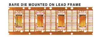 efore the die are
encapsulated, they are mounted on to lead frames, and thin gold wires connect
the bonding pads on the chip to the frames to create the electrical path
between the die and lead fingers.
efore the die are
encapsulated, they are mounted on to lead frames, and thin gold wires connect
the bonding pads on the chip to the frames to create the electrical path
between the die and lead fingers.
Product samples are taken out of the normal product flow for environmental and reliability assurance testing. These quality assurance tests push chips to their extreme limits of performance to ensure high-quality, reliable die and to assist engineering with product and process improvements.
During Encapsulation, lead frames are placed onto mold plates and heated. Molten plastic material is pressed around each die to form its individual package. The mold is opened, and the lead frames are pressed out and cleaned.
Electroplating is the next process where the encapsulated lead frames are “charged” while submerged in a tin/lead solution. The tin/lead ions are attracted to the electrically charged leads to create a uniform plated deposit which increases the conductivity and provides a clean consistent surface for surface mount applications.
In Trim & Form, lead frames are loaded into trim-and-form machines where the leads are formed step by step until finally the chips are severed from the frames. Individual chips are then put into antistatic tubes for handling and transportation to the test area for final testing.
Each memory chip is tested at various stages in the manufacturing process to see how fast it can store or retrieve information, including the high temperature burn-in in Micron’s proprietary AMBYX® ovens which test the circuitry of each chip, ensuring the quality and reliability. This monitored burn-in provides feedback throughout the process, allowing identification and correction of manufacturing problems.
The completed packages are inspected, sealed, and marked with a special ink to indicate product type, date, package code, and speed.
Memory Module Manufacturing Part 4
Once memory chips are made, we still need a way to connect them to your computer. To do this, the chips are mounted to printed circuit boards (PCBs). The final assembled product is called a memory module.
Micron engineers design memory modules using Computer Aided Design (CAD) programs. Module sizes will vary depending on the chip’s configuration (SIMM, DIMM, Memory type, etc.). Chip configuration also determines the electrical characteristics of the PCB.
The PCB is a critical part of the memory module. It enables your computer to access the memory. For this reason, Micron engineers place significant effort on correctly designing the PCB. Each design is tested by simulation and undergoes multiple design improvements prior to release for production.
P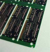 CBs are
built in arrays, or sheets, made up of several identical boards. After
assembly, the array will be separated into individual modules, similar to how
a chocolate bar can be broken into small squares. By varying the total number
of PCBs in each array based on size, Micron maximizes the number of modules
made from a given amount of raw materials. The Micron Design Engineering group
also interacts frequently with system manufacturers’ engineers to optimize the
design process and improve manufacturability of the customer’s modules.
CBs are
built in arrays, or sheets, made up of several identical boards. After
assembly, the array will be separated into individual modules, similar to how
a chocolate bar can be broken into small squares. By varying the total number
of PCBs in each array based on size, Micron maximizes the number of modules
made from a given amount of raw materials. The Micron Design Engineering group
also interacts frequently with system manufacturers’ engineers to optimize the
design process and improve manufacturability of the customer’s modules.
When the module design is perfected and the PCBs produced, memory module assembly begins! Assembly entails an intricate soldering procedure that attaches memory chips to the PCB.
Throughout the entire module assembly process, Micron takes great precaution to eliminate electrostatic discharge (ESD), or what most of us refer to as static electricity. ESD damage is a leading cause of device failure. That same “shock” you feel after shuffling your feet across carpet then touching something can completely destroy a memory chip. In fact, a person passing within 12 inches of an unprotected chip can cause damage. Micron team members wear protective clothing and use anti-static equipment during the assembly process. This ensures that any electrical charges on people or equipment will not transfer to the memory modules. Additionally, after every manufacturing step, the product is checked and verified and in-line Statistical Process Control (SPC) data is gathered. These checks provide immediate feedback to ensure continuous improvement.
Memory Module Manufacturing Part 5
The first step in assembling the memory module is Screen Print. A stencil is used to screen solder paste onto PCBs. The stencil ensures the solder paste affixes only where components will attach. Solder paste is tacky and holds chips in place on the PCB. If a chip is misplaced, it can be removed and the solder paste is cleaned off the board.
P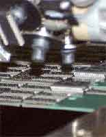 CBs contain several marks
called fiducials. These are not part of the circuit but are locators for
placing chips. Vision systems in High Speed Automated Pick and Place machines
scan the fiducials to dimensionally check and locate where to place chips on
PCBs. Pick and Place machines are programmed to know which chips are placed
where. The machine picks a chip from the feeder and places it in its
appropriate location on the board. The same process occurs for all remaining
chips and for any other components on the module. Of all the steps your memory
module goes through, this is the fastest. All the chips are placed on a PCB in
just a few seconds!
CBs contain several marks
called fiducials. These are not part of the circuit but are locators for
placing chips. Vision systems in High Speed Automated Pick and Place machines
scan the fiducials to dimensionally check and locate where to place chips on
PCBs. Pick and Place machines are programmed to know which chips are placed
where. The machine picks a chip from the feeder and places it in its
appropriate location on the board. The same process occurs for all remaining
chips and for any other components on the module. Of all the steps your memory
module goes through, this is the fastest. All the chips are placed on a PCB in
just a few seconds!
Next, the assembled chips and boards pass through an oven. The heat melts, or reflows, the solder into a liquid stage. When the solder cools, it solidifies, leaving a permanent bond between chips and board. The surface tension of the molten solder prevents the chips from misaligning during this process.
Once the chips are attached, the array is separated into individual modules. Micron team members visually inspect each module. Many modules also undergo additional inspections using automated X-Ray equipment to ensure no unreliable solder joints exist. All Micron Memory Modules meet IPC-A-610 acceptance criteria - the industry standard recognized worldwide.
Micron then tests and tags the modules. We use custom equipment to automatically test performance and functionality. This eliminates any possibility of an operator mistakenly placing a failed module in a passing location. Certain modules are programmed with an identifying “Dog Tag” that your PC will recognize and read.
Finally, the modules are sampled through one last Quality Inspection. They are placed into ESD safe plastic trays or bags and are ready for delivery. Finished product is shipped to the customer. Micron is the memory supplier to the top PC manufacturers in the world.
Final Product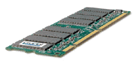 Who else
manufacturers memory?
Who else
manufacturers memory?
There are only a handful of “true” manufacturers of memory - that is,
companies who fabricate the memory chips. These manufacturers sell their chips
mostly to major computer manufacturers for use in their systems. In the memory
upgrade market, however, there are a number of vendors who claim to be memory
manufacturers, but the truth is, these vendors buy the memory chips from a
manufacturer like Micron, then, merely assemble the modules. Other vendors in
the upgrade market simply buy the modules from a manufacturer, repackage them,
and sell them under their brand name.
No Comments Yet
Leave a Comment